PCB: from Concept to design to fabrication and testing using Fritzing.
A detailed description of how I created a PCB - and the lessons learned.
LEDs and Buttons and shift registers, oh my!
I have been having loads of fun designing boards and having these boards fabricated for next to nothing. Let me explain how.
In a previous blog post -- My First Homemade PCB (or: Why Next Time I'm Ordering My PCB Online) -- Amir wrote about his experience learning Eagle, the preferred ECAD tool for professionals. Since Eagle requires an expensive licensing fee, I researched other options.
Because it’s free and designed for hobbyists, I decided on Fritzing. Fritzing lets you go all the way from breadboard design, to schematic design, to board layout, and even to board fabrication. In addition, I’ve found a board house that fabricates 10 small boards for $5 -- pcbway.com.
With this new found knowledge, I now am ready to take many of my breadboard designs and “complete” them by fabbing a PCB.
Let’s start with the following two circuits: a test of shift registers along with their compatibility to Arduino SPI and/or shiftin/shiftout.
LEDs & SHIFT OUT Register, 74595
First, here is a breadboard for a SHIFT OUT circuit. It uses the 74595 to receive serial bits and light up 8 LEDs. You may recognize this circuit as a standard exercise to learn the proper operation of the 74595 while also illustrating how to expand the I/O ports on the Arduino. This is well documented in the Arduino Learning section -- Serial to Parallel Shifting-Out with a 74HC595.
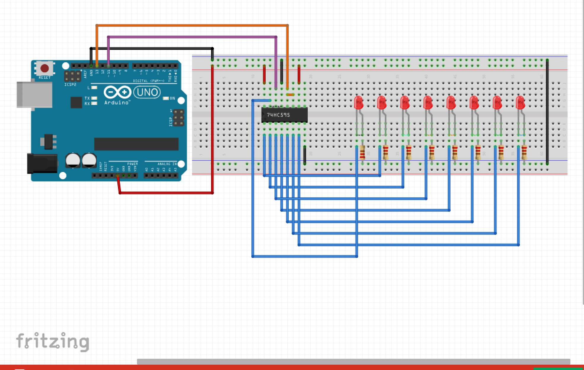
In Arduino C, the code to send an 8-bit value to the 74595 chip is simply
void write_shift_regs(byte value)
{
    digitalWrite(Latch_Pin, LOW);
    shiftOut(MOSI_Pin, SCLK_Pin, MSBFIRST, value);
    digitalWrite(Latch_Pin, HIGH);
}
Buttons & SHIFT IN Register, 74165
Second, here is a breadboard of a SHIFT IN circuit, wherein the 74165 chip buffers the buttons and then sends those values serially to the Arduino.
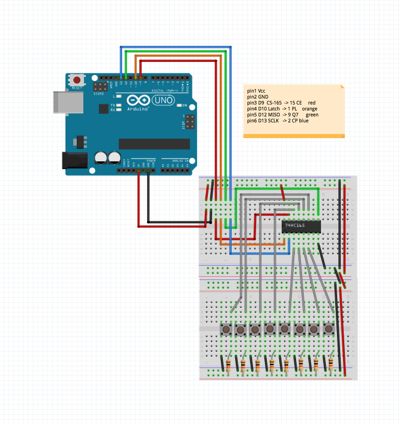
In Arduino C, the code to receive an 8-bit value from the 74165 chip is simply
byte read_shift_regs()
{
    // pulse LOAD to latch the data lines,
    digitalWrite(loadPin, LOW);
    delayMicroseconds(PULSE_WIDTH_USEC);
    digitalWrite(oadPin, HIGH);

    // read the bit values from the 74HC165, using a shiftIn
    byte bitValues = shiftIn(dataPin, clockPin, LSBFIRST);

    return (bitValues);
}
For an extra-fun challenge, I combine both of these circuits onto a single Arduino Shield. The 74595 and 74165 together are connected to the Arduino with only 5 signals:
- SCLK (Serial Clock)
- MISO (Master In Slave Out)
- MOSI (Master Out Slave In)
- STORE (LED’s 74595 8-bit buffer store)
- LOAD (Button’s 74165 8-bit buffer load)
This is as signal efficient as true SPI-compatible devices.
Arduino Shield
I decided to build this circuit as an Arduino shield, a relative small form-factor (54mm x 69mm), but with built-in paths to all the Arduino digital signals.
It will be an excellent challenge to get all components onto this small form-factor.
Breadboard
The combined breadboard for this is:
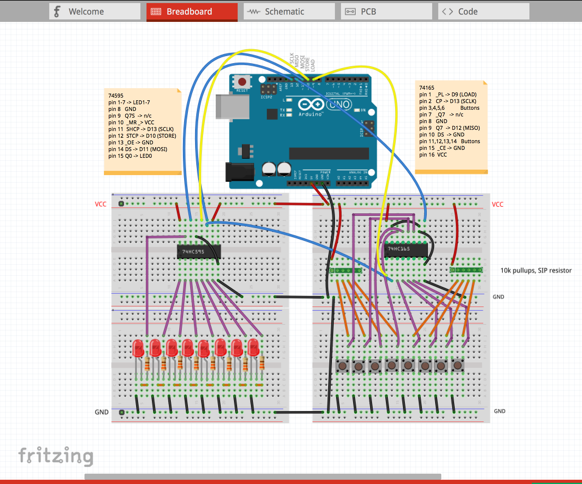
This is an image from the Fritzing design – I started to actually wire-up this on a real breadboard and quickly lost patience. The promise of a quicker PCB fabrication lured me to skip that step. Although I didn't build this breadboard, Fritzing provides you the tools to document your design extremely well.
I recommend that you use all the features of Fritzing at the breadboard design stage. The most helpful features are: wires of different colors, note boxes, and text labels. Wires may be drawn straight, or with 90° bends, or with arcs. In combination, the circuit can be drawn very clearly.
Schematic
Next, we draw the combined schematic. This step is fairly easy, because Fritzing places all the components in your drawing spaces, and draws dotted-lines, called “ratsnest wiring”, between all the connections required.
We just need to straighten out the components and organize the wires a bit:
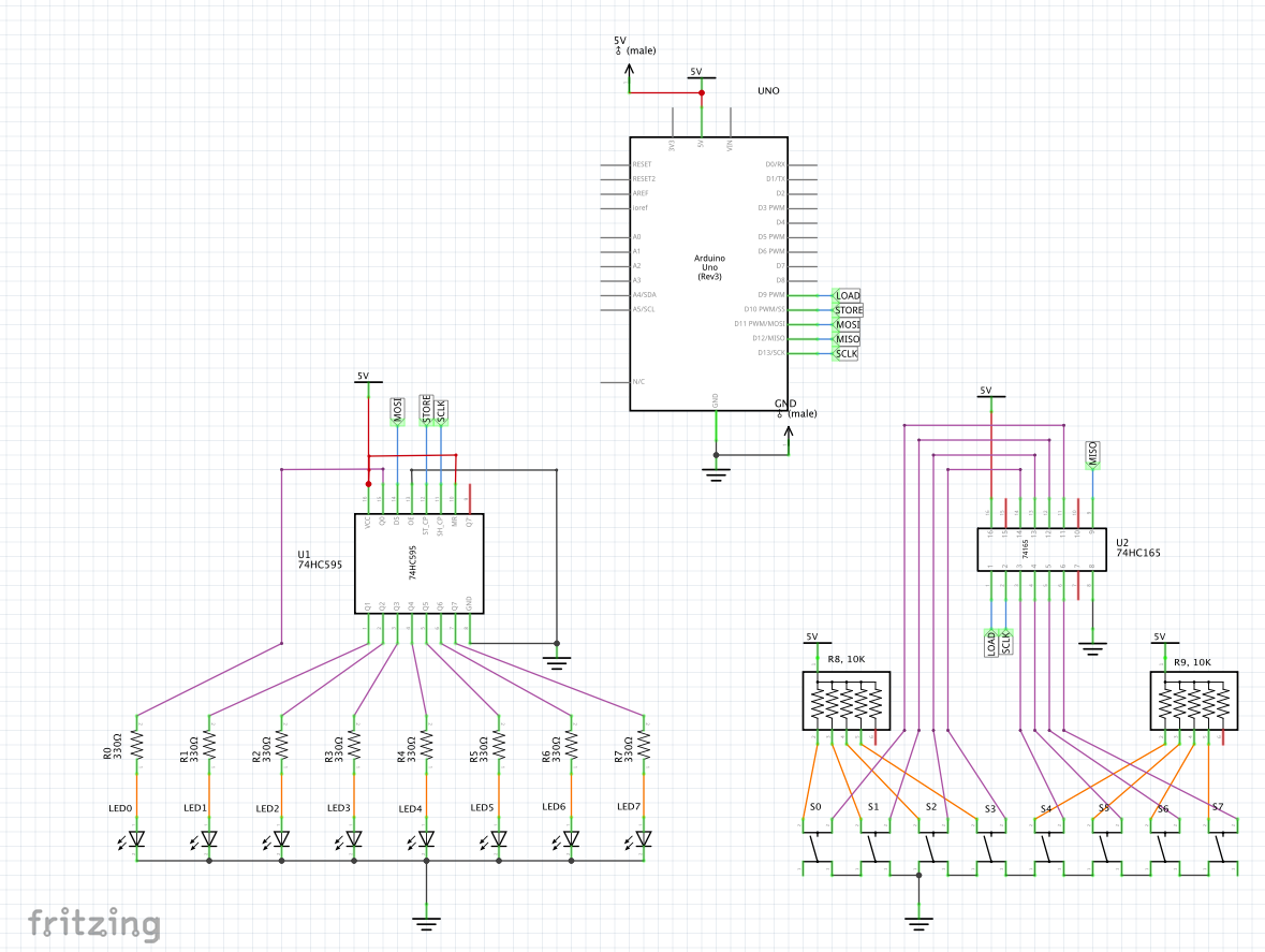
I recommend that you use the following features of Fritzing at the schematic design stage.
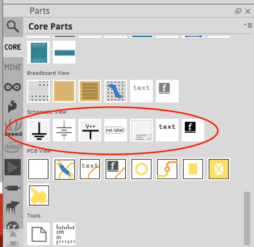
These include: connections of different colors (similar to the breadboard view), text, GND and Vcc labels and net labels. Net labels are similar to variable names in C, but for hardware design. The judicious and careful use of net labels can greatly enhance the clarity of your schematic. In the above example, my net labels are:
LOAD, STORE, MOSI, MISO, and SCLK.
Notice that connections may be drawn straight or with various bends. In combination, the circuit can be drawn very clearly.
PCB Layout
Next step, start the PCB layout. I was unfamiliar with this module so I started with a simpler problem – the layout of the 8 LEDs, and 1 chip on the board.
I then added the 8 buttons and the next chip.
A problem arose with Fritzing. When you duplicate a lot of parts, the parts can be placed in the view you are in -- Breadboard, Schematic, or PCB – but in a jumbled mess in the other views. I found it necessary to start over and add only a few components at a time. By doing so, the components were placed correctly in all three views.
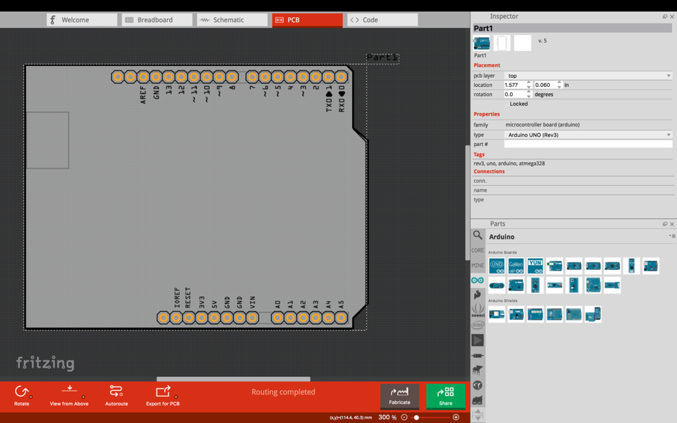
Start with the PCB the shape of an Arduino Shield. Then add the Arduino Uno pins.
Next we add 8 LEDs and 8 Buttons. Hmm… quite a lot of effort is required to line them up and space them out evenly.
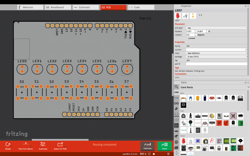
Next, add the pullup resistors and the current-limiting resistors. Finally, add the IC’s.
Notice that there is not a lot of room left to run the traces.
After each step, I visited the Schematics view and the Breadboard view, and placed the components where I wanted them.
Finally, I ran all the wires, in the breadboard view and in the schematic view.
Running traces in the PCB view is the arduous task. It required significant time and trial and error to find the best way to run the traces.
I had to do all the routing by hand. The Fritzing Autorouter really does an ugly job, and ultimately fails with many unrouted traces.
To save space, I turned the resistors up on-end.
I had to reduce the size of nearly all traces, except VCC and GND, from 24mil to 16mil. Since then, I have learned that 10mil is perfectly adequate for all signal traces.
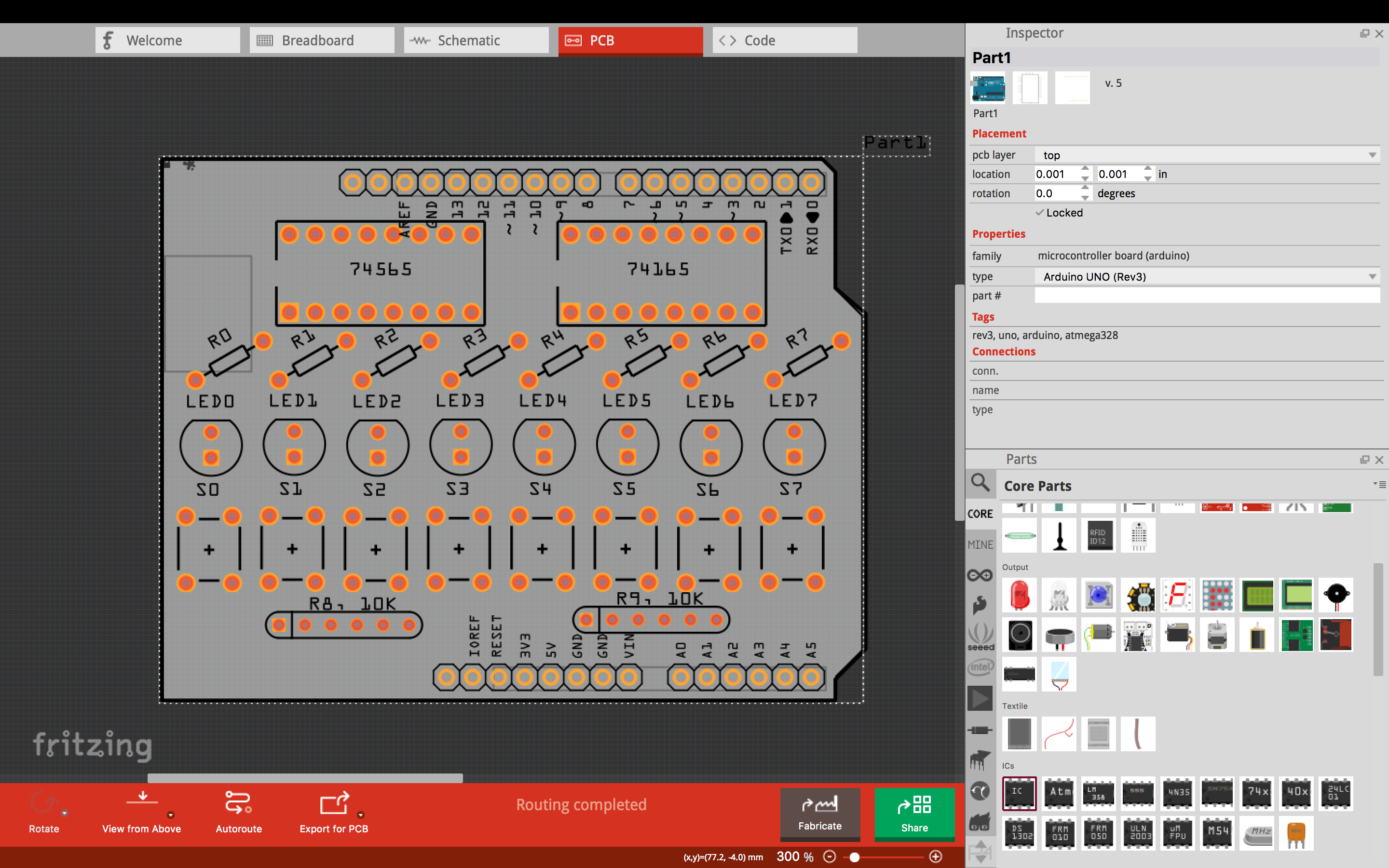
Finally, the PCB design was complete.
Version 1.0 board
Below is the PCB image of this board.
There are only 4 VIAs. A VIA is the path between the upper copper layer and the lower copper layer. It took considerable work and imagination to perfect the paths and minimize the VIAs. Notice how dense the traces are above LED 2,3,4 …
Fritzing doesn’t have good tools for this. I had to drag and position each trace by hand in order to achieve that density.
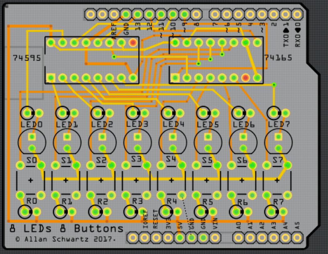
There is one error on the board, indicated by the dashed line between GND and one of the legs of a switch. It turns out I omitted one ground signal. More about this later…
Production
Next I placed my order to PCBWAY, submitted the files and waited.
PCBWAY keeps you abreast of the process on your order status page:
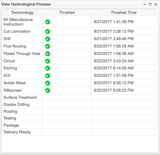
I submitted three different boards to fabricate. Within a couple of days, my boards arrived!
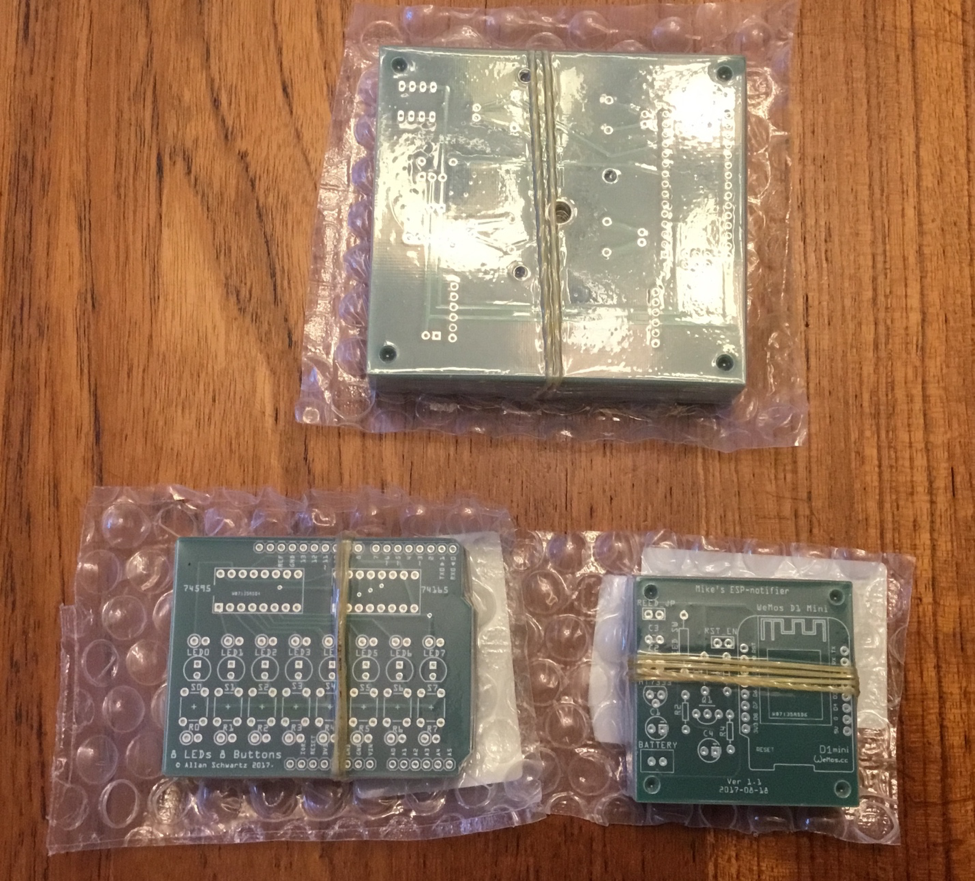
Assembly
Next we assemble the boards
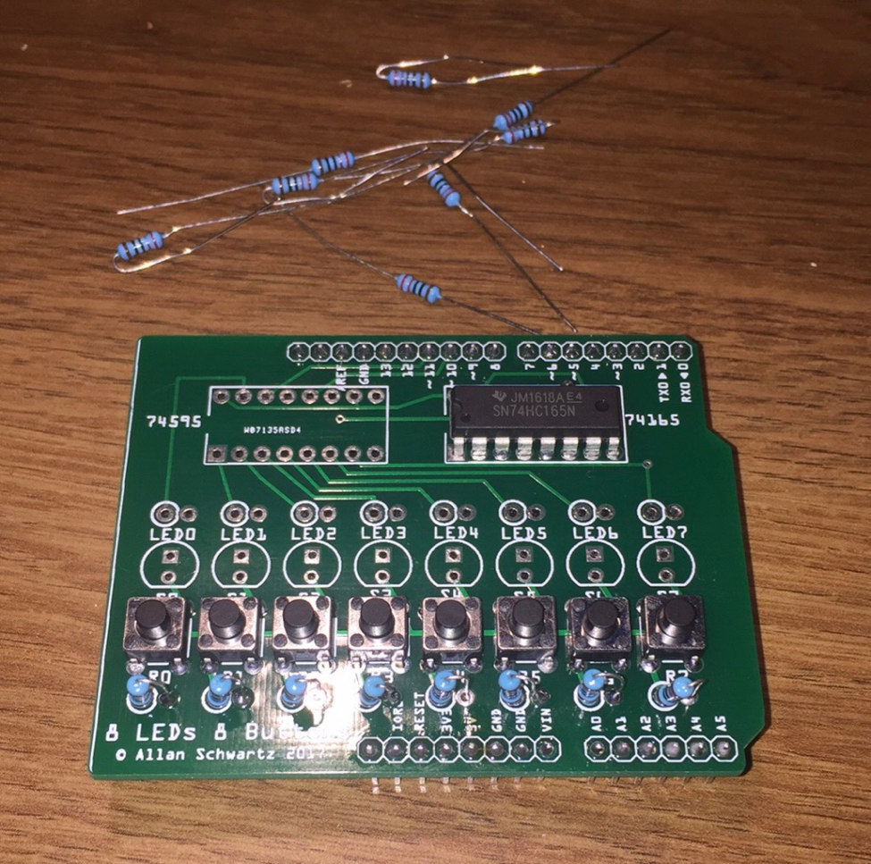
I built up the first half of the board to debug the 74165 connections. Unfortunately, the circuit did not work.
Hardware Debugging
I immediately started debugging the problem, using my Saleae 8-port logic analyzer.
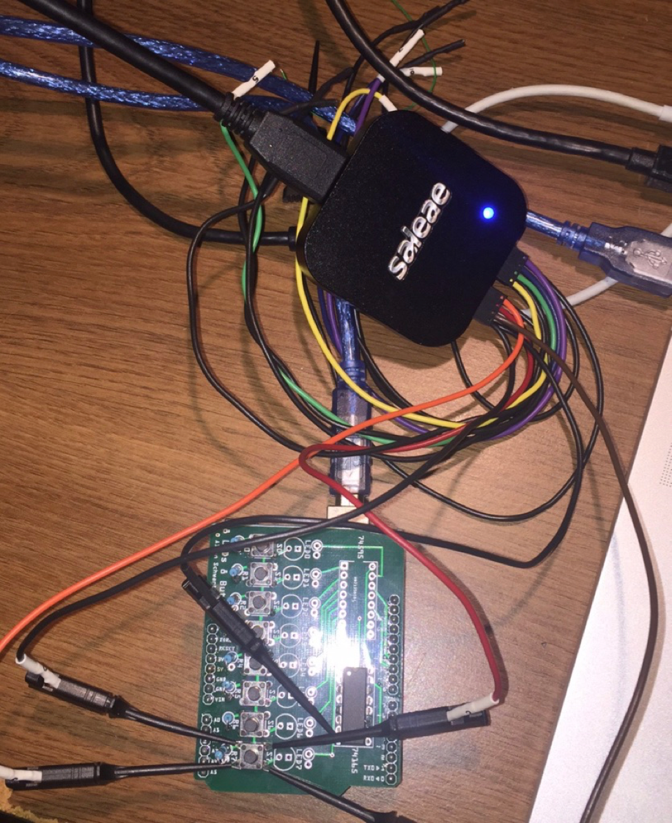
The Saleae Logic Analyzer turns my Mac Book Pro screen into a sophisticated signal analyzer. After one brief capture, I identified a problem: pins on the switch legs were floating.
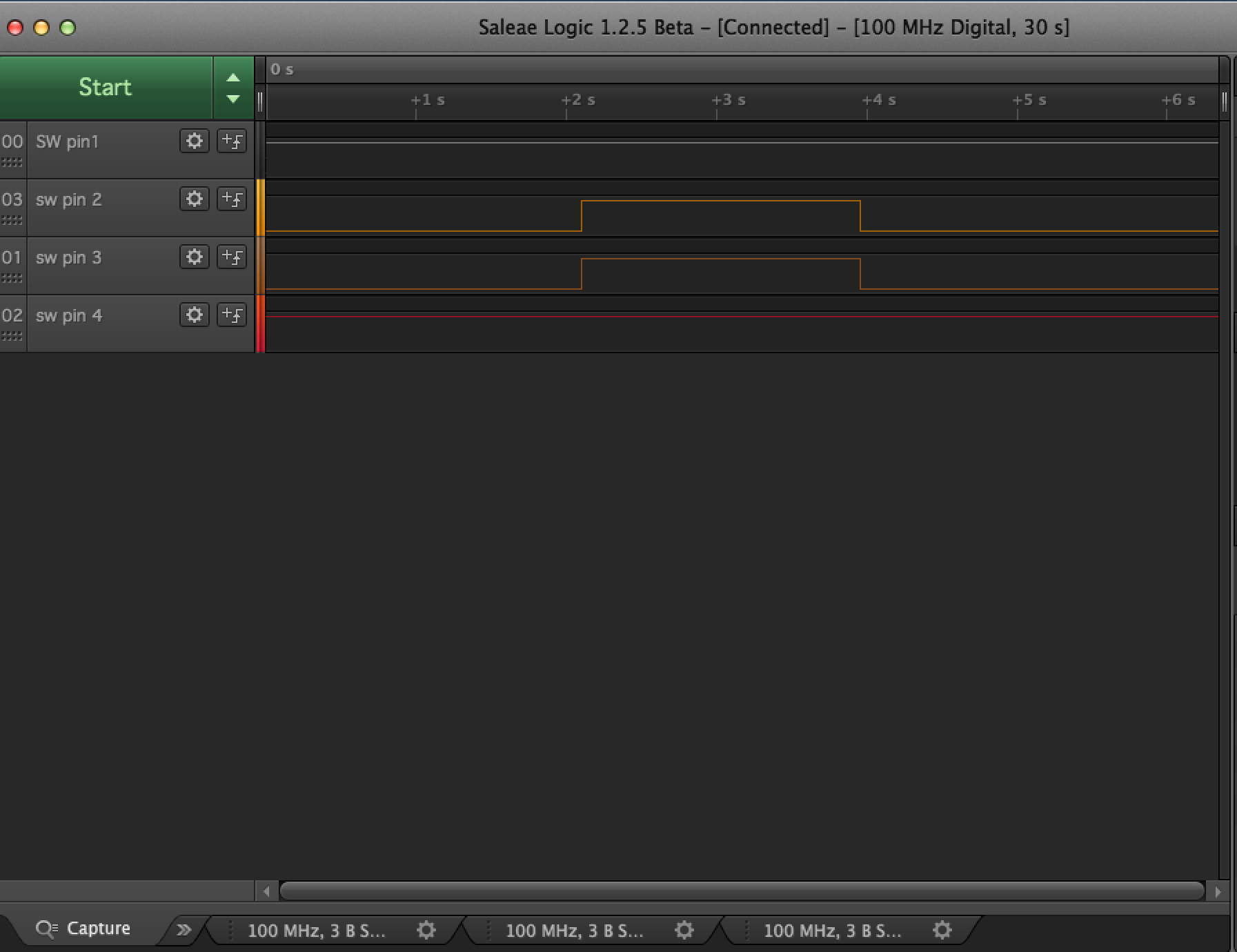
It turns out that I had omitted one ground signal. After rotating the switches so they would fit better, I think that I lost track of which switch leg corresponded to which signal.
This diagram should explain that mystery:
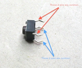
Once I understood the switches common legs, I realized that I was wiring all the switches wrong.
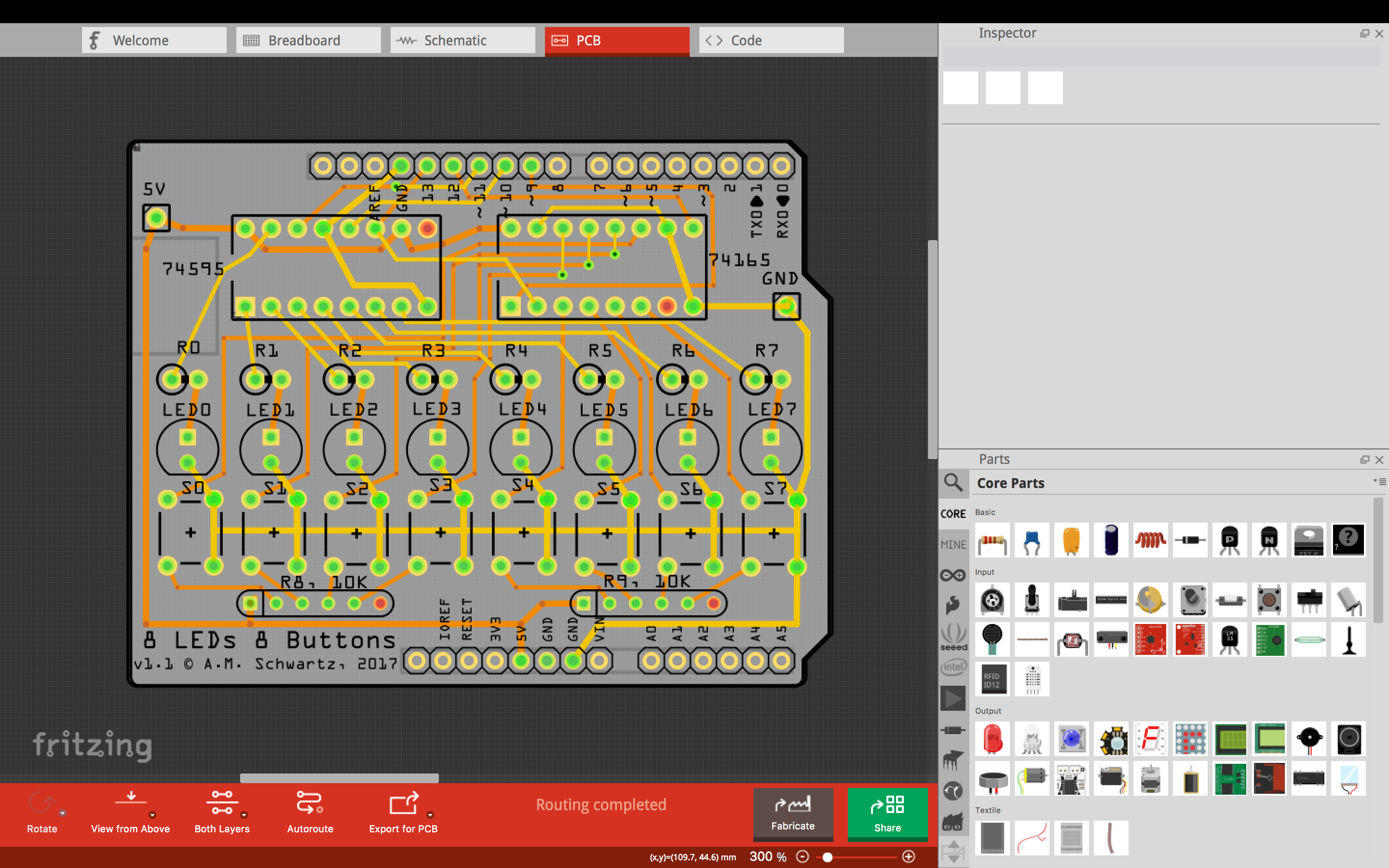
Final Version 1.1 board
So, back to layout. I connected one pair of the common legs of a switch just to remind myself that they are connected. I also remembered I had SIP resistors, which take up much less board space, so I used those. Here is my v1.1 board:
I reordered from PCBWAY, received the new PCBs, and assembled the first one.
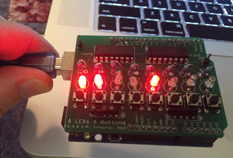
After some minor adjustments to the software, it works perfectly!
Lessons learned:
- The 74165 does not perfectly emulate the SPI protocol.
- The 74595 and 76165 together can be hooked up to the Arduino with only 5 signals.
- Hardware isn’t always easy: it requires debugging and iteration, just like software.
- Careful engineering processes lead to the best results.
- It is more fun to design a PCB and also less tedious to solder components, compared to hand-wiring a breadboard when the number of connections is large. This board had 80 or 90 connections.
- Fritzing is most powerful when used to Breadboard, capture Schematics, and layout PCBs in tandem.
Fritzing is an efficient tool to fabricate very nice PCBs. At least for us Hobbyists.
Postscript
Since publishing this blog, I have designed a few more boards. See my next blog for how I designed a PCB for a Desktop NeoPixel Clock.